| About | SS&S | Music | Anime | 3D | Wallgames | Betsubetsu | Others... |
| SY99 Disk | FM Tutorial | Effects | My Music | Programming |
| Belt | Suppliers | Adapter |
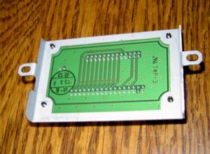
| Socket adapter board | ||
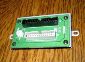 |
The replacement drive used in the Yamaha replacement drive kit has a different pinout on its ribbon cable, so this tiny new board is used as an adapter. By examining this circuit board it is possible to see how the conversion from 26 pins to 34 pins (plus two pin power cable) is accomplished. First, let's compare the 26 and 34 pin connectors: |
| 26-way Floppy Ribbon | /=active low | |
| Pin No. | Signal Name | Description |
| 1 | VCC | VCC +5V |
| 2 | /INDEX | Index |
| 3 | VCC | VCC +5V |
| 4 | /DRVS | Drive Select |
| 5 | VCC | VCC +5V |
| 6 | /DSKCHG | Disk Change |
| 7 | RES | Reserved |
| 8 | READY | Ready |
| 9 | MEDIA | Media |
| 10 | /MOTE | Motor Enable |
| 11 | /REDWC | Density Select |
| 12 | /DIR | Direction |
| 13 | RES | Reserved (In Use) |
| 14 | /STEP | Step |
| 15 | GND | Ground 0V |
| 16 | /WDATE | Write Data |
| 17 | GND | Ground 0V |
| 18 | /WGATE | Write Gate |
| 19 | GND | Ground 0V |
| 20 | /TRK00 | Track 00 |
| 21 | GND | Ground 0V |
| 22 | /WPT | Write Protect |
| 23 | GND | Ground 0V |
| 24 | /RDATA | Read Data |
| 25 | GND | Ground 0V |
| 26 | /SIDE | Side 1 Select |
| 34-way Floppy Ribbon | /=active low | |
| Pin No. | Signal Name | Description |
| 1 | GND | Ground 0V |
| 2 | /REDWC | Density Select 1=Low, 0=High |
| 3 | GND | Ground 0V |
| 4 | N/C | - |
| 5 | GND | Ground 0V |
| 6 | N/C | - |
| 7 | GND | Ground 0V |
| 8 | /INDEX | 0=Index |
| 9 | GND | Ground 0V |
| 10 | /MOTEA | Motor Enable 0=Drive 0 |
| 11 | GND | Ground 0V |
| 12 | /DRVS1 | Dirive Select 1 |
| 13 | GND | Ground 0V |
| 14 | /DRVS0 | Drive Select 0 |
| 15 | GND | Ground 0V |
| 16 | /MOTEB | Motor Enable 0=Drive 1 |
| 17 | GND | Ground 0V |
| 18 | /DIR | 0= Direction Select |
| 19 | GND | Ground 0V |
| 20 | /STEP | 0= Head Step |
| 21 | GND | Ground 0V |
| 22 | /WDATA | Write Data |
| 23 | GND | Ground 0V |
| 24 | /WGATE | Floppy Write Enable, 0= Write Gate |
| 25 | GND | Ground 0V |
| 26 | /TRK00 | 0= Track 00 |
| 27 | GND | Ground 0V |
| 28 | /WPT | 0= Write Protect |
| 29 | GND | Ground 0V |
| 30 | /RDATA | Read Data |
| 31 | GND | Ground 0V |
| 32 | /SIDE1 | 0= Head Select |
| 33 | GND | Ground 0V |
| 34 | /DSKCHG | S1= Disk Change, 0= Ready |
| By compairing the functional names, it is possible to see how the same controls are passed across the two interfaces. Note that the 26 pin socket has VCC present, and so only one ribbon cable is required. For a 34 pin socket, then no VCC is present, and so a separate cable needs to be made to provide VCC +5V, and Ground to the floppy drive. This is the extra white non-IDC socket that you can see on the adapter board above. NOTE: these pinouts should make it very clear that it is NOT possible to connect a 34 pin floppy drive directly into a 26 pin socket (or vice-versa) - and doing this could damage both the SY99 and the floppy drive. It is now possible to construct a table showing which pins to connect to which pins to make an adapter (pins are split into functional groups): |
| Yamaha XS051 Adapter PCB | /=active low | X=NO | /=active low | |
| Signal | 26-way Pin No. | Linked? | 34-way Pin No. | Signal |
| VCC +5V | 1 | X | 1 | Ground 0V |
| VCC +5V | 3 | X | 3 | Ground 0V |
| VCC +5V | 5 | X | 5 | Ground 0V |
| Reserved | 7 | <-> | 7 | Ground 0V |
| MEDIA | 9 | <-> | 9 | Ground 0V |
| /REDWC | 11 | <-> | 11 | Ground 0V |
| Reserved | 13 | <-> | 13 | Ground 0V |
| GND | 15 | <-> | 15 | Ground 0V |
| GND | 17 | <-> | 17 | Ground 0V |
| GND | 19 | <-> | 19 | Ground 0V |
| GND | 21 | <-> | 21 | Ground 0V |
| GND | 23 | <-> | 23 | Ground 0V |
| GND | 25 | <-> | 25,27,29,31,33 | Ground 0V |
| /INDEX | 2 | <-> | 8 | /Index |
| X | 10 | /Drive Select 0 | ||
| /DRVS | 4 | <-> | 12 | /Drive Select 1 |
| /DSKCHG | 6 | X | ||
| /MOTOR ENABLE | 10 | <-> | 16 | /Motor On |
| /DIR | 12 | <-> | 18 | /Direction Select |
| /STEP | 14 | <-> | 20 | /Step |
| /WDATA | 16 | <-> | 22 | /Write Data |
| /WGATE | 18 | <-> | 24 | /Write Gate |
| /TRK00 | 20 | <-> | 26 | /Track 00 |
| /WPT | 22 | <-> | 28 | /Write Protect |
| /RDATA | 24 | <-> | 30 | /Read Data |
| /SIDE1 | 26 | <-> | 32 | /Side Select |
| READY | 8 | <-> | 34 | /Ready |
| VCC +5V | 1,3,5 | X | Separate cable and connector | VCC +5V |
| Ground | Many | X | Separate cable and connector | Ground 0V |
|
After having done all this investigative work, this table was then compared with the Yamaha adapter board supplied with the replacement Yamaha drive, and it appeared to be identical. It was then tested by a volunteer in Russia (successfully!)... I then found this link from FM-Alive's web-site, which serves as validation - Note: this link downloads a zip file containing a Word file, which some users may not be able to read easily... |
||
 |
Useful background information
|
| Note: | This is my own description of what I did with my SY99, and is shown here as an illustration of how an ex-service engineer approaches this type of task. If you attempt to make an adapter or adapter board of any kind then you do so entirely at your own risk. You should only attempt this type of activity if you are suitably qualified, and confident of your ability to complete the task successfully. I am not suggesting that you should make these modifications at all - I am merely documenting my hardware and providing a hypothetical example. These pages are not authorised or endorsed by Yamaha in any way. You should always refer any servicing enquiries to your local Yamaha Dealer, or your country's Yamaha Service Department. |
| Back to the main description page... |
| About | SS&S | Music | Anime | 3D | Wallgames | Betsubetsu | Others... |
| SY99 Disk | FM Tutorial | Effects | My Music | Programming |
| Belt | Suppliers | Adapter |
 |
| © 2004-2008 Martin Russ |